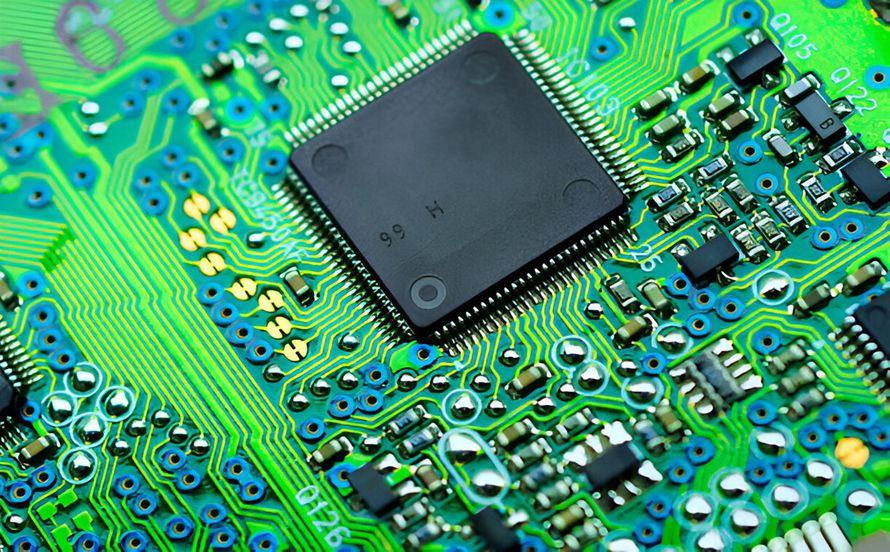
A microvia PCB is a critical technology in modern electronics, enabling high-density interconnections and compact circuit layouts that traditional PCB designs cannot support. As electronic devices continue to become smaller, faster, and more powerful, engineers increasingly rely on microvia PCBs to achieve higher routing density, improved signal integrity, and better overall performance. From smartphones and wearables to aerospace and medical devices, microvia PCBs play a vital role in next-generation electronics.
This article explains what a microvia PCB is, how it is manufactured, its advantages, applications, and why choosing the right microvia PCB manufacturer is essential for consistent quality and reliability.
What Is a Microvia PCB?
A microvia PCB is a printed circuit board that uses very small vias, typically with a diameter of less than 150 microns, to connect different layers of the board. Unlike conventional through-hole vias, microvias are usually laser-drilled and are most commonly used in high-density interconnect (HDI) PCB designs.
Microvias allow designers to place components closer together and route signals more efficiently between layers. They can be blind vias, buried vias, or stacked and staggered microvias, depending on the complexity of the design. This technology enables thinner boards, higher layer counts, and more compact electronic assemblies.
Structure and Types of Microvia PCB
The structure of a microvia PCB is similar to a standard multilayer PCB but with advanced interconnection features. Microvias typically connect only adjacent layers, reducing signal path length and electrical loss.
Blind microvias connect an outer layer to an inner layer without passing through the entire board. Buried microvias connect inner layers only and are not visible from the surface. Stacked microvias are placed directly on top of one another to connect multiple layers, while staggered microvias are offset to improve reliability.
The choice of microvia structure depends on design density, electrical requirements, and manufacturing capability.
Microvia PCB Manufacturing Process
The manufacturing process of a microvia PCB is more complex than standard PCB fabrication and requires specialized equipment and expertise. The process begins with laminate preparation and imaging of circuit patterns on individual layers.
Laser drilling is used to create microvias with high precision and minimal material damage. After drilling, the vias are cleaned and plated with copper to ensure reliable electrical connections. For multilayer HDI designs, sequential lamination is performed, building the board layer by layer.
Each step must be carefully controlled to maintain alignment, plating quality, and structural integrity. Final inspection and electrical testing verify continuity, insulation resistance, and overall board performance.
Advantages of Microvia PCB
One of the primary advantages of a microvia PCB is increased routing density. Smaller vias free up valuable board space, allowing more traces and components within a limited area. This is essential for compact devices such as smartphones and wearable electronics.
Microvia PCBs also offer improved electrical performance. Shorter signal paths reduce inductance and capacitance, resulting in better signal integrity and lower noise. This makes microvia technology ideal for high-speed and high-frequency applications.
Another key benefit is reduced board thickness. By eliminating large through-hole vias, microvia PCBs enable thinner and lighter designs, supporting modern product form factors.
Microvia PCB vs Traditional Through-Hole PCB
Traditional through-hole vias pass through the entire thickness of the PCB, occupying space on every layer and limiting routing flexibility. In contrast, microvia PCBs use targeted interconnections that preserve routing space and improve layout efficiency.
While through-hole PCBs are simpler and more cost-effective for low-density designs, microvia PCBs are essential for advanced electronics where size, performance, and reliability are critical. The choice depends on design complexity, volume, and application requirements.
Applications of Microvia PCB
Microvia PCBs are widely used in consumer electronics such as smartphones, tablets, laptops, and smartwatches. These products require high-density layouts and excellent signal performance in extremely compact spaces.
In the telecommunications industry, microvia PCBs support high-speed networking equipment, base stations, and data communication systems. Automotive electronics, including advanced driver-assistance systems and infotainment modules, also rely on microvia PCBs for compact and reliable designs.
Medical devices, aerospace systems, and industrial automation equipment benefit from microvia PCBs due to their precision, reliability, and ability to support complex circuitry.
Design Considerations for Microvia PCB
Designing a microvia PCB requires careful planning and adherence to manufacturing guidelines. Via size, aspect ratio, and pad design must be optimized to ensure reliable drilling and plating. Stacked microvias require special attention, as they are more prone to stress and fatigue if not designed correctly.
Material selection is also important. High-quality laminates with good thermal and mechanical stability help prevent delamination and via failure. Signal integrity, power distribution, and thermal management must be carefully balanced in dense HDI layouts.
Close collaboration with a manufacturer during the design phase can significantly improve yield and reduce production risks.
Quality Standards and Testing for Microvia PCB
Quality control is especially critical for microvia PCBs due to their small feature sizes and complex structures. Automated optical inspection and X-ray inspection are commonly used to verify via alignment, plating quality, and internal connections.
Electrical testing ensures continuity and insulation resistance across all layers. Thermal cycling and reliability testing may be performed to validate long-term performance under operating stress.
A qualified manufacturer follows strict process controls and international standards to ensure consistent quality in microvia PCB production.
How to Choose the Right Microvia PCB Manufacturer
Choosing the right microvia PCB manufacturer is essential for achieving reliable and scalable production. Manufacturing capability should include advanced laser drilling, sequential lamination, and precise plating control.
Experience with HDI and microvia technology is equally important. A skilled manufacturer can provide design for manufacturability support, helping optimize layouts for performance and cost efficiency.
Strong quality management systems, transparent communication, and flexible production capacity are key indicators of a reliable long-term partner.
Future Trends in Microvia PCB Technology
As electronic devices continue to evolve toward higher performance and smaller form factors, demand for microvia PCBs is expected to grow. Emerging technologies such as 5G, artificial intelligence hardware, and advanced medical electronics require increasingly dense and precise PCB designs.
Advancements in laser drilling, materials, and inspection technologies are enabling even smaller microvias and higher layer counts. These innovations ensure microvia PCBs remain at the forefront of electronic manufacturing.
Conclusion
A microvia PCB is a foundational technology for high-density, high-performance electronic designs. By enabling compact layouts, improved signal integrity, and reduced board thickness, microvia PCBs support the most advanced electronic products on the market today.
To ensure consistent quality, precise fabrication, and dependable performance, partnering with an experienced microvia PCB manufacturer is the key to successfully bringing complex HDI designs into production.


